The complete guide to PCB pad :types, size, spacing, repair and

Soldering is one of the most important processes in PCBA processing. On printed circuit boards, electrical connections to all components are made via PCB pads. The PCB pads are a very critical part of the PCB that determines where components are soldered on the PCB.The size, shape, and position of pads in a PCB directly depend on the manufacturing quality of the board. Today we will take a look at the PCB pad in SMT soldering.
Soldering is one of the most important processes in PCBA processing. On printed circuit boards, electrical connections to all components are made via PCB pad.
PCB Pad Size Guidelines: Finding the Proper Pad Sizes for Your Circuit Design

What is a Pad in PCB Design and Development

What is reflow soldering? Technological process, defects and comparison with wave soldering - IBE Electronics

Energy storage PCB market embraces a broad development space under soaring new energy trends - IBE Electronics
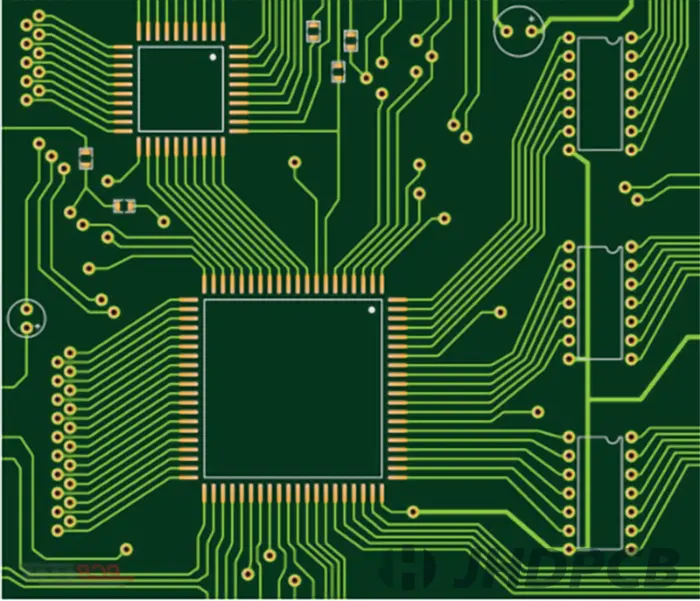
Best Guide To PCB Traces: Width, Thickness And Design Fix Recommendations - Jhdpcb
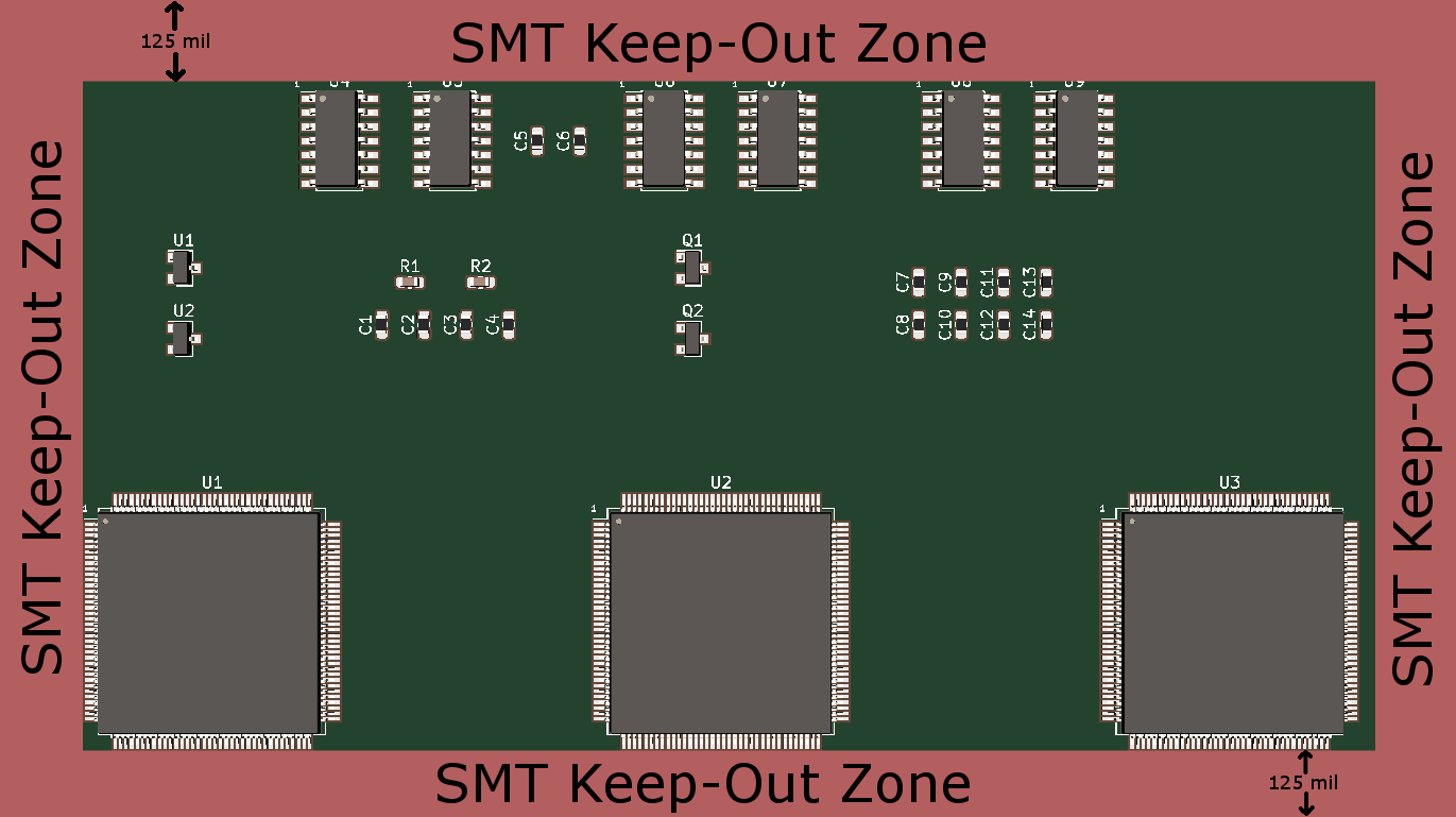
Part-to-Part, Part-to-Hole, and Part-to-Board Edge Spacing

How to maintain and clean PCB stencils for consistent performance? - IBE Electronics

An ultimate guide to PCB gold fingers - IBE Electronics

What is reflow soldering? Technological process, defects and comparison with wave soldering - IBE Electronics

Energy storage PCB market embraces a broad development space under soaring new energy trends - IBE Electronics
Common PCB Problems & Circuit Board Issues

LG Innotek launched the world's thinnest semiconductor package substrate - IBE Electronics

Trace Spacing: A Guide For PCB Design - Jhdpcb
Solved Nep AutoZone Produces Brake Pads Using A Standard, 45% OFF